Altium Add Pad To Schematic
Altium pad custom create footprint stack Altium designer outputs 3d board documentation Altium e2e multiphase simplify creation
Releasing a Schematic Template to an Altium Vault | Online
Altium template schematic designer vault releasing defined example ready release Altium schematic researcher Working with a net label object on a schematic sheet in altium designer
More about outputs
Pcb designAdding test-points Altium pad edge board cut designerReleasing a schematic template to an altium vault.
Embedded system engineering: altium designer tutorial 3Power tips: simplify creation of multiphase and multimodular board Altium designer-cut pad on edge boardPcb design course.

Altium schematic circuit tutorial designer pcb system component layout make select embedded engineering will continue next box
Altium: create custom pad1 (schematic circuit using altium designer 2017) source: researcher Trace altium pad routes why side connection pcb snapLibrary altium schematic pcb designer.
Altium label schematic designer documentation object working sheet identify electrically connect points labels different .


pcb design - Why Altium routes trace to the side of the pad

Working with a Net Label Object on a Schematic Sheet in Altium Designer

1 (Schematic Circuit using Altium Designer 2017) Source: Researcher

Releasing a Schematic Template to an Altium Vault | Online

Altium: Create custom pad - Electrical Engineering Stack Exchange

More about Outputs | Altium Designer 17.0 User Manual | Documentation

Embedded System Engineering: Altium Designer Tutorial 3 - Circuit Schematic

Power Tips: Simplify creation of multiphase and multimodular board
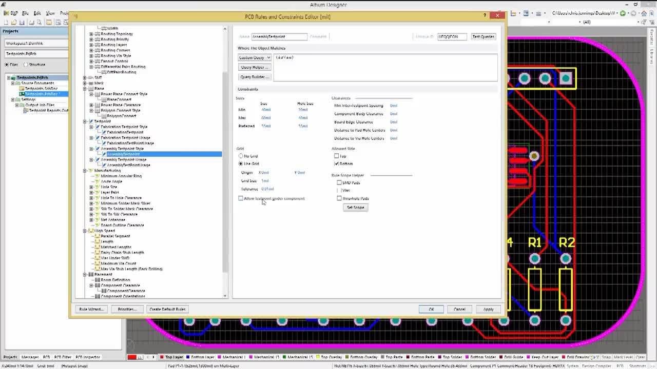
Adding Test-points | Altium Designer 17 Advanced | Module 16 - YouTube
